The semiconductor industry is engaged in a relentless race where the aim is high integration, high density and miniaturisation of logic devices. This has resulted in the development of new technologies such as 3D ICs that make it possible to integrate extensive functionality into ever smaller, faster and lower power consumption devices. However, these more complicated integrated circuits require more sophisticated tools for development and prototyping, inspection and failure analysis in order to analyse or reach the areas of interest.
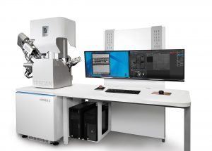
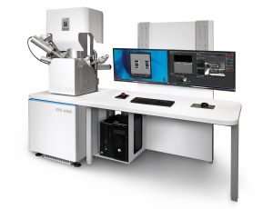
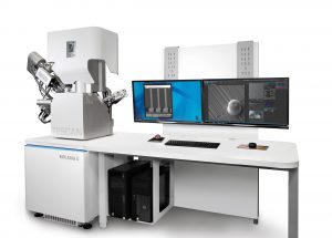
TESCAN AMBER X
Optimized plasma FIB-SEM platform for high-quality deprocessing of the most modern semiconductor devices with proprietary chemistries
More information