- Low-kV high-resolution imaging with enhanced topographic contrast of target layers
- Imaging of edges of delayered or cleaved chips using field-free high-resolution technology
- Dedicated and proprietary gas chemistries for sub-14 nm nodes deprocessing
- End-pointing software module for semiautomated deprocessing enables stopping the process at a desired layer
- Electrical characterization of the most sensitive semiconductor devices using in-situ nanoprobing
- Easy-to-use, fully customizable, applicationoriented and modular user interface
-
-
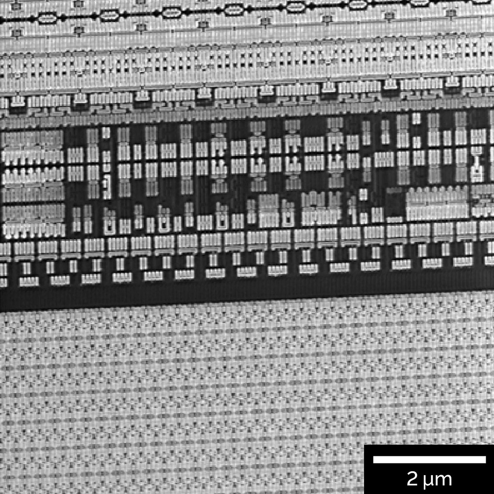
TCL layer, Intel 14 nm Skylake
-
-
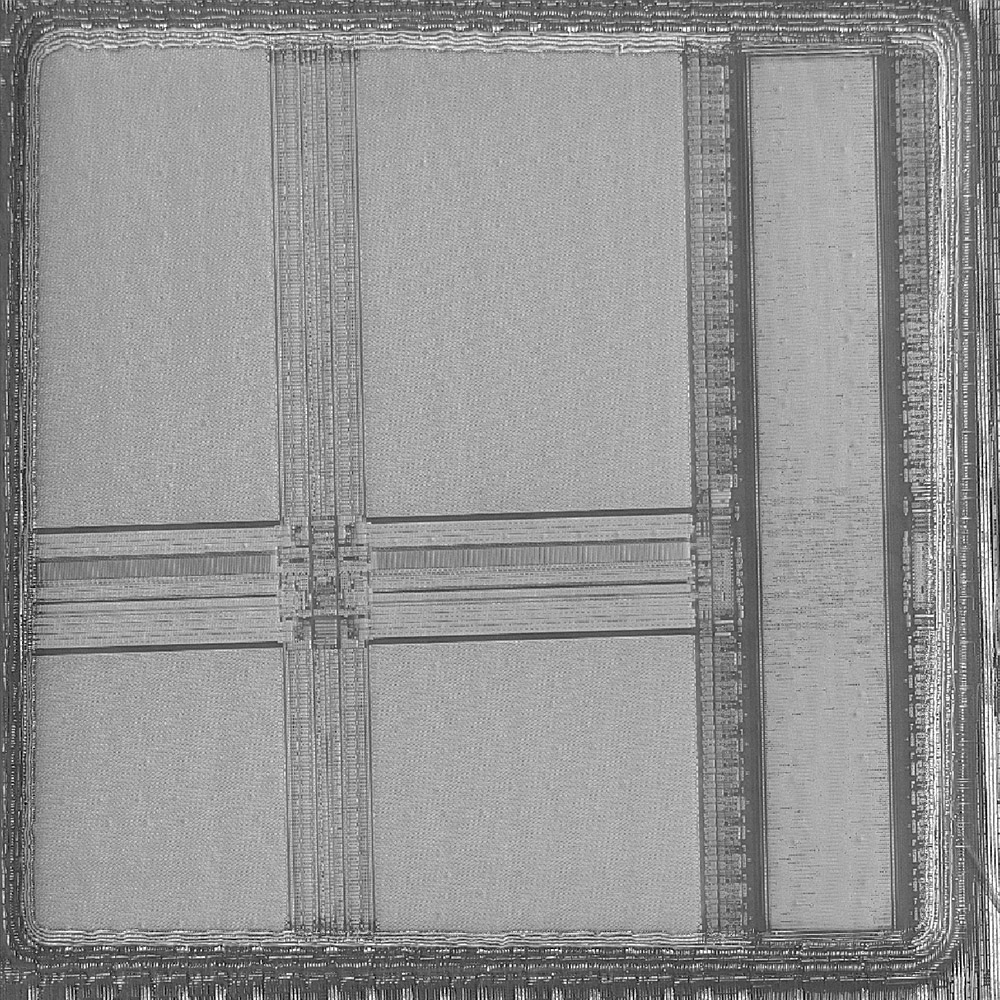
Overview of a 100 μm × 100 μm delayered window on a 10 nm technology node
-
-
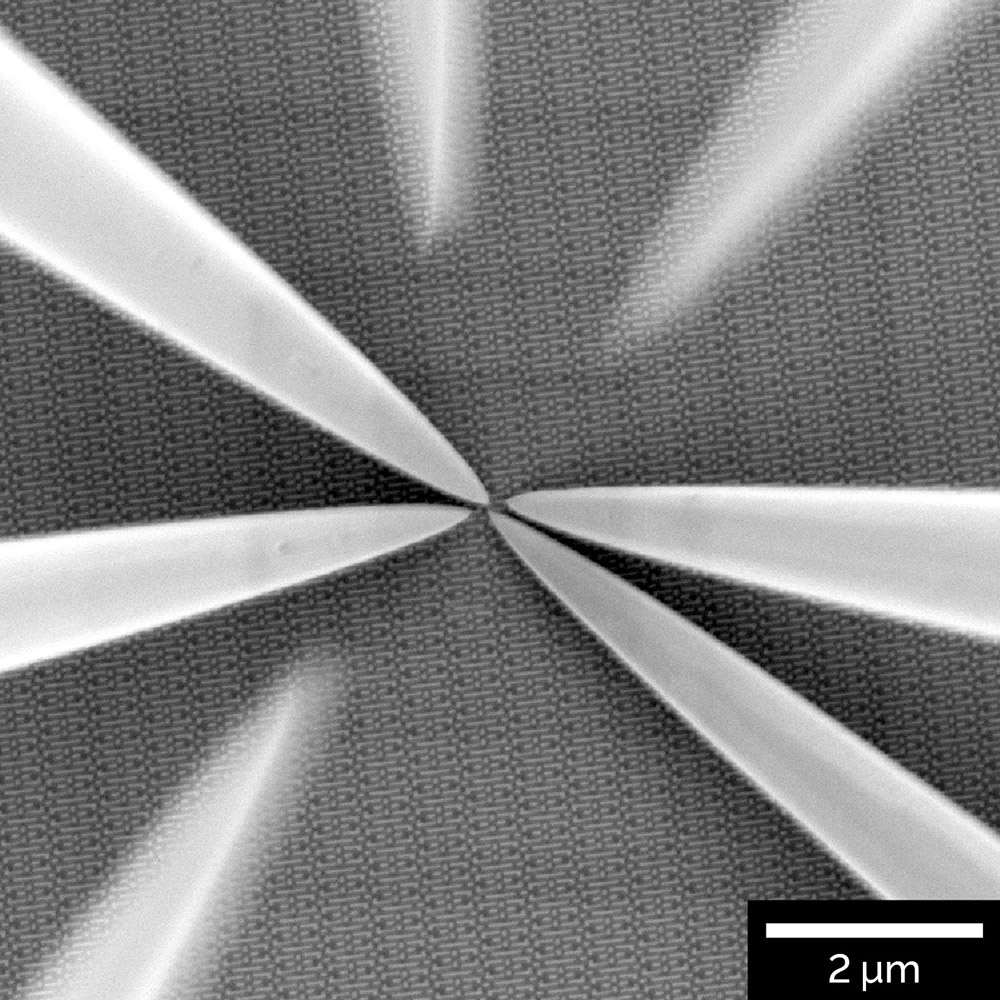
Nanoprobing a delayered
10 nm technology node